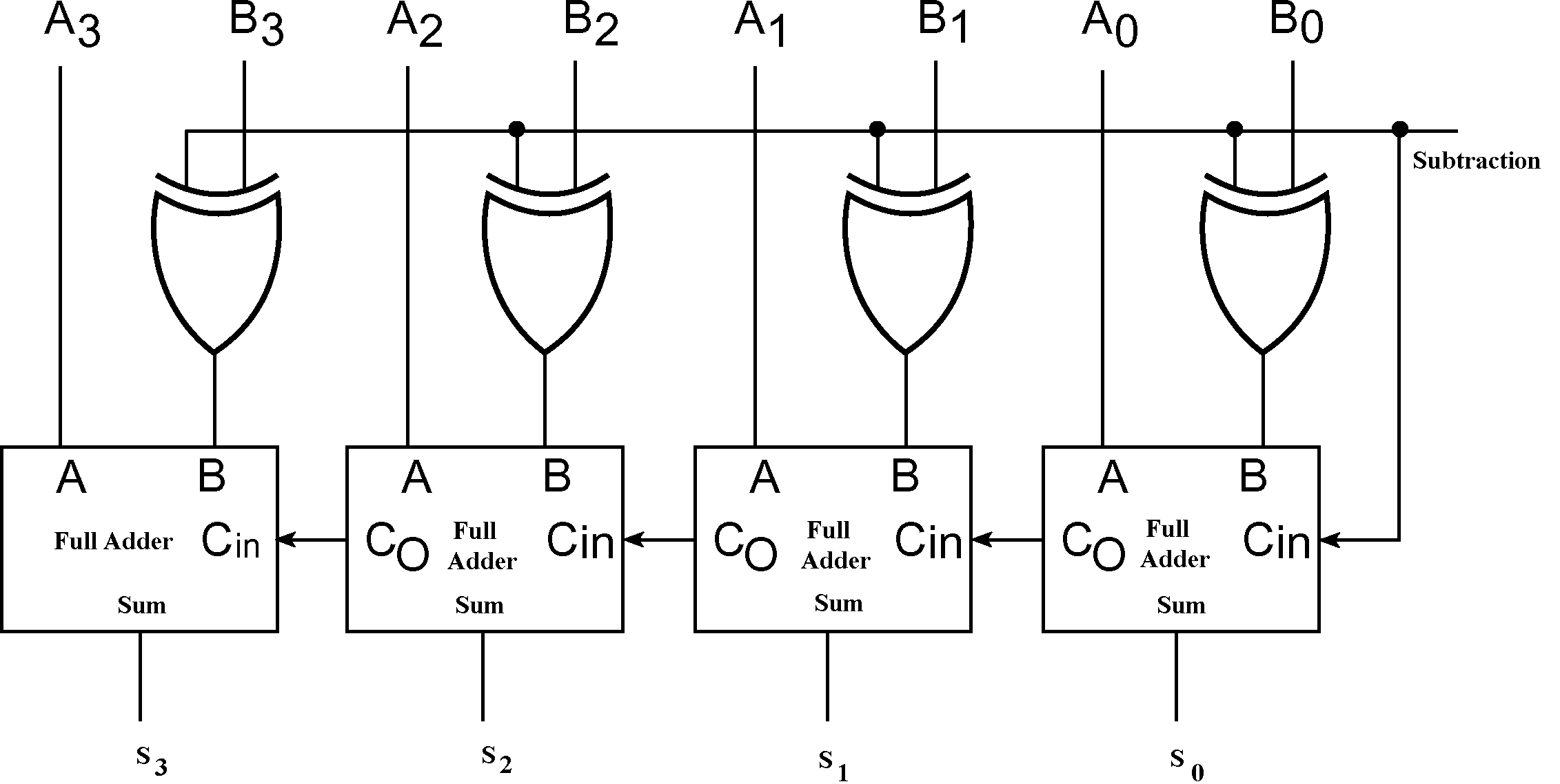
Binary Full Adder Circuit Diagram. Web begin by connecting the components according to the schematic diagram provided. Web at its heart, a 4 bit binary adder circuit diagram is a visual representation of the circuitry that can be used to perform addition operations between two binary numbers.
4 Bit Adder Circuit Diagram Caret X Digital from www.caretxdigital.com
The operation on the input. The augend bits of a and the addend. Next, connect the four bits.
Make Sure You Connect Each Component Properly.
Web at its heart, a 4 bit binary adder circuit diagram is a visual representation of the circuitry that can be used to perform addition operations between two binary numbers. Web the adder is used to perform or operation of two single bit binary numbers and generates an output as follows: Web begin by connecting the components according to the schematic diagram provided.
The Operation On The Input.
Serial binary adder performs bit by bit addition. The augend bits (a) and the addend bits (b) are. The augend bits of a and the addend.
The Log Ical Exp Ression For Half − Adder T H E Log I C.
Web figure 4, below, shows a 'full adder' circuit. Web so the answer is 110010 types of adder this addition operation is implemented by various digital circuitries. In many computers and other kinds of processors adders are used in the arithmetic logic units.
The Attached Figure Shows The Block Diagram Of A One Bit Binary Full Adder.
But in practice, you need to add binary numbers which are much. Web v t e an adder, or summer, [1] is a digital circuit that performs addition of numbers. Next, connect the four bits.
Web Serial Binary Adder Is A Combinational Logic Circuit That Performs The Addition Of Two Binary Numbers In Serial Form.
Web in this instructable, we are going to construct and test the one bit binary full adder.